FVME2TM, FVME2TMWR
Contents
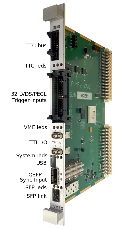
FVME2TM is a Trigger, Timing and Control Module for VMEDAQ system. It is a successor of TTCM module. It is a 6U VME64x slave module. FVME2TM has onboard 41.667 MHz clock generator that is used for clock source for TTC bus. FVME2TM has TTL level LEMO inputs for spill and trigger signals and 32 ECL/LVDS inputs for trigger signals. Two TTL level LEMO outputs are software programmable. TTL inputs has 50 Ohm internal termination. TTL outputs are capable of driving 50 Ohm load.
FVME2TMWR is a FVME2TM board with White Rabbit support.
Front Panel Interfaces

Inputs/Outputs
- LEMO 1 - SPILL input. External sync signal, positive logic. Readout enabled with logic one on this input.
- LEMO 2 - TRIG input, 5 ns minimum
- LEMO 3 - lemo_XOFF input OR programmable output1
- LEMO 4 - programmable output2
- LVDS1..LVDS32 - Trigger inputs, LVDS or ECL, 5 ns minimum
Status LEDs
FVME2TM front panel has 12 LEDs with the following layout:
LEDs |
Function |
||
G |
Y |
R |
trig read, trig block, spill |
G |
Y |
R |
vme run, vme activity, vme error |
G |
Y |
R |
|
G |
Y |
R |
SFP leds |
VME Interface
VME Interrupt Lines
- IRQ1 - data read XOFF input
VME Registers
Detailed description of TTCM VME Registers
VME Data Format
Clock and Synchronization
Trigger Cable
For use with TQDC-16, special ribbon twisted pair cable is supplied with 34-pin connector on one side and four 10-pin connectors on other side. One cable connects four TQDC-16 modules with TTCM.
Input Aggregation
Trigger inputs are combined after shaping and delay by OR scheme. 40 inputs are reduced to 4 trigger lines. Logic OR is performed this way (trigger line = input OR input ...):
- ST = LVDS1
- TQDC1 = LVDS6 | LVDS10 | LVDS14
- TQDC2 = LVDS18 | LVDS22 | LVDS26 | LVDS30
- NIM = NIM1 | ... | NIM7
Trigger Logic Delay
Measured delay from NIM input to TTC bus output: min. 530 ns, max. 580 ns. Due to 20 MHz sampling the delay is varied by 50 ns. this applies to TTCM firmware 1.0.10604
TTC Bus
TTC connector pinout
pin pair |
signal |
description |
1, 2 |
spill |
Trigger and data readout enable |
3, 4 |
parity |
Odd parity of spill and trigger signals |
5, 6 |
trigger |
Trigger signal |
7, 8 |
clock |
41.667 MHz clock signal |
9, 10 |
ground |
TTC bus signal ground |
Even signal pin positive.
Spill, trigger and parity signals have width 50 ns and are synchronous to clock.
Connector: 2.54 mm 2x5 (10 pins).
Connector part numbers: AMP - 1658621-1
Signal Timing
measurement |
min |
typ |
max |
|
clock frequency |
|
41.666667 MHz ±0.001% |
|
|
spill, parity, trigger |
setup time, ns |
|
8.5 |
10.0 |
hold time, ns |
5.0 |
6.0 |
|
|
Timing provided by design TTCM v2.0 firmware rev.8512
1 ns step

CLK  ___/^^^^^^^^^\_________/^^^^^^^^^\_________/^^^

TRIG ________XXXXXXX^^^^^^^^^^^^^XXXXXXX__________...

                    | setup |hold|
TTC 2.0 Timecode Extension
Spill signal is used as a gate for data acquisition. Trigger signal is used only when spill signal is active.
In order to provide TAI timecode to modules an extension of TTC standard is proposed, TTC 2.0.
With spill signal low, trigger line become an encoded serial data channel, 40 Mbps data rate. Timecode information is transmitted serially using 8b10b encoding and K28.5 comma symbol as idle code. Big endian byte order. A sequence of data coded forms a frame.
TAI timecode is encoded as TAI 64-bit Timestamp.
Frame Type 1: Timecode
Frame type 1 transmission time: 25 ns * 20 words * 10 bit = 5 µs. The moment of beginning of first bit of frame corresponds to TAI timecode data being transferred.
Byte |
|
0 |
Frame type |
1 |
TAI seconds [39:32] |
2 |
TAI seconds [31:24] |
3 |
TAI seconds [23:16] |
4 |
TAI seconds [15:8] |
5 |
TAI seconds [7:0] |
6 |
TAI nanoseconds [29:22] |
7 |
TAI nanoseconds [21:14] |
8 |
TAI nanoseconds [13:6] |
9 |
TAI nanoseconds [5:0], flags[1:0] |
10 |
spill_id[31:24] |
11 |
spill_id[23:16] |
12 |
spill_id[15:8] |
13 |
spill_id[7:0] |
14 |
reserved |
15 |
reserved |
16 |
CRC32[31:24] |
17 |
CRC32[23:16] |
18 |
CRC32[15:8] |
19 |
CRC32[7:0] |
- TAI - International Atomic Time
- flags[3:0] = {time_valid, ptp_wr_mode, ptp_mode, ntp_mode}
- CRC32 use Ethernet 802.3 polinom

